HTRB, HTGB and H3TRB Test Systems for Power Semiconductors
Verify junction integrity and oxide reliability under extreme conditions
Overview
Our HTRB test systems verify the long-term reliability of power semiconductors under extreme conditions — high temperature, high voltage, humidity. The systems run autonomously for 1,000 hours and more, monitor each device individually and document the entire test history. Three test methods target different weak points.
HTRB — Reverse voltage under sustained stress
The device is stressed at 150 – 230 °C with its maximum reverse voltage. Over 1,000 hours, it becomes clear whether the junction remains stable or leakage currents increase. Typical weak points: contamination on the chip surface, defects in the edge termination and aging of the passivation. Our system continuously measures the leakage current of every single channel — anomalies are detected immediately.
HTGB — Gate oxide under stress
This test targets the gate oxide rather than the blocking junction: maximum gate voltage at maximum temperature. The test reveals whether the device's turn-on threshold shifts over time. For SiC devices in particular, this test is critical — the interface between SiC and gate oxide is more sensitive than in silicon and reacts more strongly to sustained stress.
With independent gate voltage sources per channel, you can run HTRB and HTGB on the same platform — without hardware reconfiguration between tests.
H3TRB — Humidity as a stress factor
The device is stressed at 85 °C and 85% relative humidity with reverse voltage. The combination of heat, moisture and electric field can cause corrosion and short circuits inside the device over months — failure mechanisms that never occur in a dry laboratory environment.
Built for continuous operation
For decades, Schuster Elektronik has been building test systems for semiconductor qualification — for module manufacturers, suppliers and test laboratories across Europe, North America and Asia. Our systems are designed for weeks of autonomous operation:
- Test voltage up to ±2,000 V (Si, SiC, GaN)
- 18 single specimens or 9 half-bridge modules per station
- Bias current measurement up to 300 mA per channel
- Temperature measurement up to 200 °C directly at the DUT
- Modular expansion to more than 10 stations
- Automatic limit monitoring with immediate shutdown
- Network interface for remote monitoring and data export
- Compliant with common qualification standards (AQG 324, AEC-Q101, JEDEC)
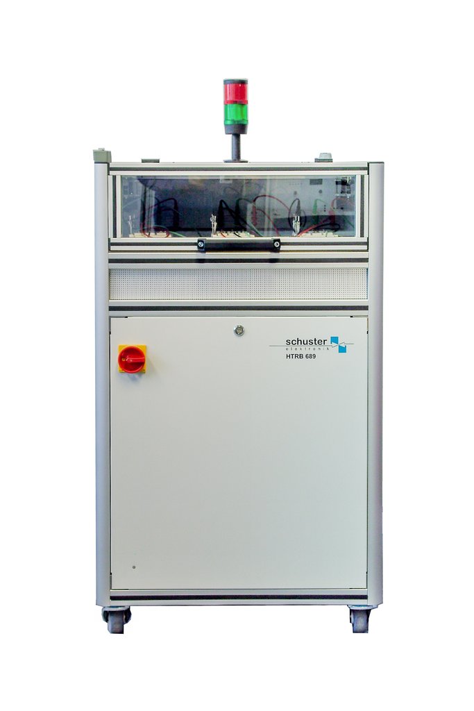
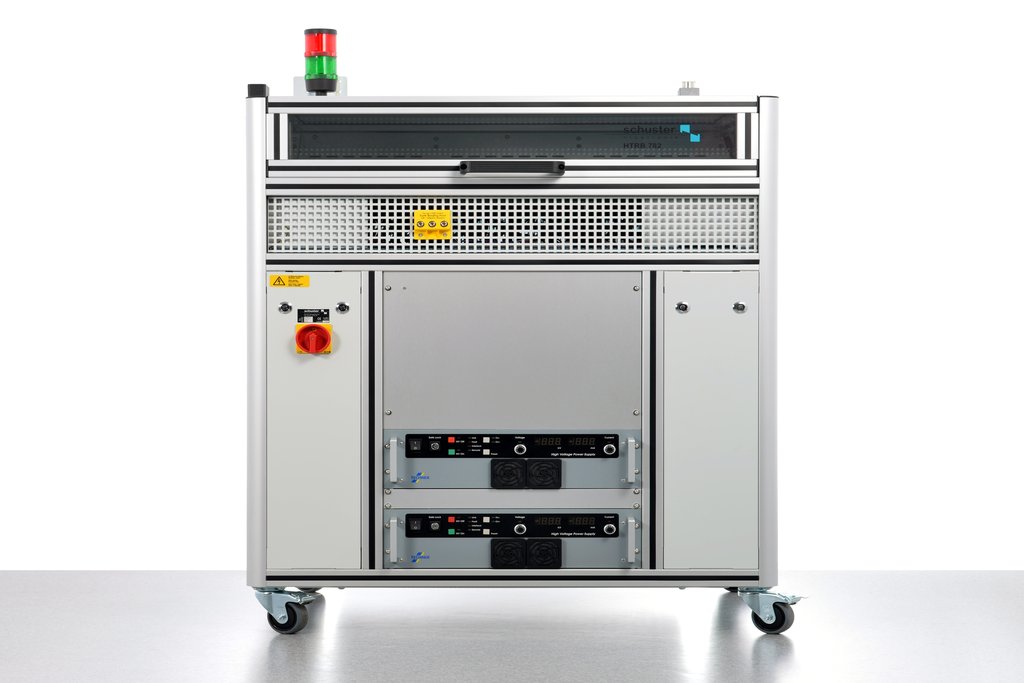
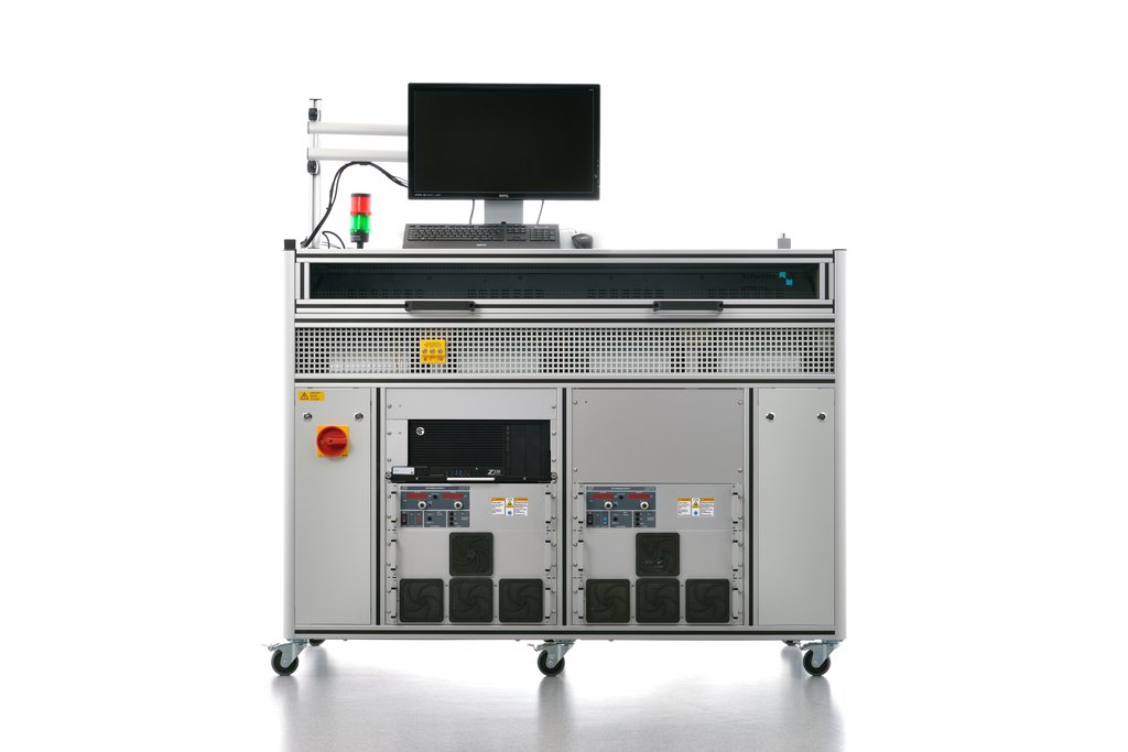
Our HTRB Test Systems
Inquiry about HTRB, HTGB, H3TRB
Interested in products or updates in the field of HTRB, HTGB, H3TRB? Contact us — we're happy to advise you.